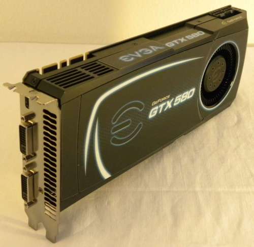
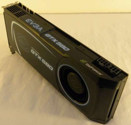
Quantcast
Channel: Overclocking | Geeks3D
Viewing all 30 articles
Browse latest View live

[GPU Tool] MSI Kombustor 1.0.6 and Afterburner 1.6.0 Beta 4

$
0
0

MSI Kombustor 1.0.6


A new version of Kombustor, MSI’s graphics card stress test tool, is available with the beta 3 and beta 4 of MSI Afterburner.

You can download the latest version of Kombustor here:
Download MSI Kombustor

Alternatively, you can download Kombustor 1.0.6 + Afterburner 1.6.0 beta 4 in the same zip package HERE.

Like Afterburner, which is a customized version of RivaTuner, Kombustor is a customized version of FurMark.

Important note: Kombustor 1.0.6 crashes when the multi-GPU version (etqw.exe) is launched on a Radeon card ( … hummm… :D ) AND when the Post Processing is checked. This bug is fixed in the version 1.0.7 and I’ll give more details on this bug when MSI will release the version 1.0.7. This bug has been reported in this thread.


[GPU Tool] MSI Kombustor 1.0.7 and OpenGL Bug with ETQW Profile

$
0
0

MSI Kombustor


A new version of Kombustor, MSI’s graphics card stress test tool (based on FurMark), is available with the beta 5 of MSI Afterburner.

You can download the latest version of MSI Kombustor here:
Download MSI Kombustor

You can also download Kombustor 1.0.7 + Afterburner 1.6.0 beta 5 in a single archive HERE.

Kombustor 1.0.7 fixes a nasty bug when it’s used with Radeon (aaahh… Radeon cards…). Actually a crash occurs when the multi-GPU version of Kombustor, etqw.exe, is executed on Radeon with recent Catalyst drivers AND with the Post-Processing enabled.

etqw.exe activates an optimizied profile in Catalyst drivers and this profile seems to change the way the OpenGL instructions are executed. When Post-Processing is enabled, Kombustor executes the following OpenGL code:

glTexImage2D(GL_TEXTURE_2D, 
             0, GL_RGBA, 
	     w, h, 
	     0, GL_RGBA, 
             GL_UNSIGNED_BYTE, 
	     NULL);

This instruction works fine every time except when Kombustor is renamed in etqw.exe.

When Kombustor is renamed in etqw.exe, glTexImage2D crashes because the last parameter is NULL (which is allowed in OpenGL – this use of glTexImage2D allows to allocate the memory for a postfx texture). The bugfix is simply to pass a valid buffer with the size of the texture….

And Kombustor 1.0.8 is still in the works..

[GPU Tool] EVGA Precision 1.9.3 Available

$
0
0

EVGA Precision 1.9.3


EVGA has released a new version of Precision, the overclocking
utility for GeForce graphics cards. EVGA Precision allows a fine tuning of the graphics card GPU core / shader and memory clocks.

To download EVGA Precision, you have to be a member of EVGA forums.
The thread about version 1.9.3 in EVGA forums is HERE.

This new version of Precision comes with a new OSD server in version 3.70. The OSD server (OSD = On Screen Display) allows to display various information (clocks, temperatures…) directly in the 3D applications.

EVGA Precision is a customized version of RivaTuner and like MSI Afterburner, EVGA Precision has a button (TEST button) that allows to launch a stress test tool. And the stress test tool is EVGA OC Scanner

[GPU Tool] MSI Afterburner 1.6.0 And MSI Kombustor 1.0.10 Available

$
0
0

MSI Afterburner 1.6.0 And MSI Kombustor 1.0.10


MSI has published the new version of Afterburner and Kombustor, MSI’s graphics cards overclocking utilities. Afterburner is the highly customized version of RivaTuner and same thing for Kombustor which is a customized version of FurMark.

You can find a detailed changelog for both tools HERE and the download is available HERE. Both tools are shipped in the same zip package.

This new version of Kombustor is essentially a bugfix release that brings a better working with Afterburner. What’s more, Kombustor 1.0.10 uses the same GPU monitoring code than GPU Shark.

The official thread for Afterburner 1.6.0 and Kombustor 1.0.10 can be found HERE @ Guru3D forums.

FurMark and Overclocked GTX 480: 108 Amperes is not a Problem…

$
0
0

FurMark and an overclocked GTX 480: 108 amperes
FurMark and an overclocked GTX 480: the intensity of the current reaches 108 amperes!

GTX 480 cooled by Thermalright's SpitFire VGA cooler
GTX 480 cooled by Thermalright’s SpitFire VGA cooler


Yes 108 amperes! A current of 108 amperes goes through the GPU. But watch out my friends, the GPU we are talking about, is the one behind the GeForce GTX 480. To reach 108A, the GPU is overclocked to 797MHz (the reference clock is 700MHz) with a VDDC (GPU voltage) of around 1.04V (the non-oc VDDC is 1V).

The guys at pcbrain.it have FurMark-ed a GTX 480 with standard clocks and VDDC and with overclocked settings. They have done the test with the stock VGA cooler and with Thermalright’s SpitFire (official page HERE).


FurMark and a GTX 480 with default settings (clocks and VDDC) and stock VGA cooler

FurMark and GTX 480 with default clocks
FurMark and a GTX 480 with default clocks and VDDC

FurMark and GTX 480 with default clocks

FurMark and GTX 480 with default clocks


FurMark and a GTX 480 with overclocked settings (clocks and VDDC) and stock VGA cooler

FurMark and overclocked GTX 480
FurMark and an overclocked GTX 480

FurMark and overclocked GTX 480

FurMark and overclocked GTX 480

FurMark and overclocked GTX 480


These images clearly show the GPU that is throttling back when temperature is too high: the temperature curve does not follow a normal heat progression. This is the overheating protection of the GTX 480.


FurMark and a GTX 480 with overclocked settings (clocks and VDDC) and Sptifire VGA cooler

FurMark and overclocked GTX 480 with a SpitFire VGA cooler
FurMark and overclocked GTX 480 with a SpitFire VGA cooler (source)

FurMark and overclocked GTX 480 with a SpitFire VGA cooler

FurMark and overclocked GTX 480 with a SpitFire VGA cooler


I did a quick test with my EVGA GTX 480 (standard settings + stock VGA cooler) and I got similar results:

FurMark and an EVGA GTX 480 with default clocks
FurMark and a EVGA GTX 480 with default clocks and VDDC

As you can see, with a good VGA cooler, an overclocked GTX 480 can resist without problem to FurMark torture stress test.

More than 100 amps for a GPU… These numbers are just impressive. I wonder if the GTX 480 can support such a current during a long period… I hope so!

[GPU Tool] Galaxy Xtreme Tuner HD v3.0

$
0
0

XTREME Tuner HD


Galaxy / KFA2 have updated Xtreme Tuner HD, their GPU monitoring and overclocking tool. Xtreme Tuner HD is like EVGA Precision / MSI Afterburner but with missing features like the GPU / memory usage. If you want to test it, you can download it HERE.

Xtreme Tuner HD works with NVIDIA cards (I tested it on an EVGA GTX 480) but no idea if it works with ATI boards too.


Update
Xtreme Tuner HD does not support ATI Radeon cards:

XTREME Tuner HD - ATI Radeon error


Thanks to Psolord for the test ;)

[via]

MSI N480GTX HydroGen: A Water Cooled GeForce GTX 480

$
0
0

MSI N480GTX HydroGen


MSI has released a new 480-core GF100 based card: the N480GTX HydroGen. This GeForce is equiped with a large full copper waterblock that covers around 70% of the PCB:

MSI N480GTX HydroGen

MSI N480GTX HydroGen

This GTX 480 comes with reference clocks (GPU: 700MHz and memory: 3696MHz QDR speed). Factory-overclocked GPU would have been nice… Anyway, water cooling is the best solution to chill a GTX 480 so all graphics cards overclockers will be happy.

This N480GTX HydroGen is priced at around… US $700.

By the way, did you already see how such a water block is made? Just watch the video in this post: Making of aquagrafx Water Block for GTX 480.

[via]

[TIPS] Radeon HD 6870 Voltage Check Points (VDDC, VDDCI and MVDD)

$
0
0

Radeon HD 6870 VDDC check points
Reading of the voltage of one phase feeding the GPU


Here is the localization of the different voltage measurement (or v-check) points on the Radeon HD 6870 PCB (back side):

Radeon HD 6870 voltage check points (2 pictures total)

Radeon HD 6870 VDDC check points


VDDC is the GPU core voltage (there are 4 x 2 points because 4 phases feed the GPU). MVDD is the memory voltage and (correct me if I’m wrong) VDDCI is the I/O bus voltage (between memory and GPU core) and comes from the PCI-Express slot.

[source]


[Tested and Burned] EVGA GeForce GTX 580 SC Review

$
0
0

EVGA GTX 580 SC 1536MB GDDR5 Review


EVGA GeForce GTX 580 SC Review Index


1 – Meet with EVGA’s GeForce GTX 580 SC

EVGA has three GTX 580 based cards in its catalog: the regular GeForce GTX 580 (with reference clocks), the GTX 580 SC, and the GTX 580 FTW Hydro Copper. Today we test the GeForce GTX 580 SC (SC for SuperClocked).

EVGA GTX 580 SC - 10 year warranty


This card, based on NVIDIA’s second generation of DX11 GPU, the GF110, comes with factory overclocked settings: a GPU clocked at 797MHz (reference: 772MHz) and 1536MB of GDDR5 memory clocked at 1012MHz real speed (reference: 1002MHz) or 4050MHz effective / QDR speed (see here for more details on memory speeds: Graphics Cards Memory Speed Demystified).

EVGA’s GTX 580 SC is a Direct3D 11 and OpenGL 4.1 capable card. In the GPU computing side, this GTX 580 support CUDA, PhysX and OpenCL 1.1.

On EVGA’s website, the GTX 580 SC is priced at USD 520$.

EVGA is well-known for it high quality support and once you have registered you card, you’ll get a 10-year warranty:

EVGA GTX 580 SC - 10 year warranty


What’s more, the registration will give you a licence key for 3DMark11 (see here for mode details: Get 3DMark 11 Advanced Edition FREE* Upon Release!).

I must say that EVGA GTX 580 SC is a very nice card. The card follows NVIDIA’s reference design but the final stickers give the card a very neat aspect. Furthermore, the packaging is well polished. We feel the bundle has been carefully prepared.

Here are some pictures of the EVGA GeForce GTX 580 SC (more pictures: EVGA GeForce GTX 580 SC Gallery – (19 pictures total)):

EVGA GTX 580 SC 1536MB GDDR5 Review

EVGA GTX 580 SC 1536MB GDDR5 Review

EVGA GTX 580 SC 1536MB GDDR5 Review


Many more BIG pictures of EVGA GeForce GTX 580 SC can be found here:

EVGA GeForce GTX 580 SC Gallery – (19 pictures total).


EVGA’s bundle includes the following components:

EVGA GTX 580 SC 1536MB GDDR5 Review

EVGA GTX 580 SC 1536MB GDDR5 Review

EVGA has also included a gaming poster in the bundle (stuck behind my testbed now!):

EVGA GTX 580 SC 1536MB GDDR5 Review


In the overclocking side, EVGA’s product offers good overclocking capabilities. What’s more, the GTX 580 SC is bundled with two overclocking utilities: EVGA Precision and EVGA OC Scanner (latest news about OC Scanner: EVGA OC Scanner @ Geeks3D):

EVGA OC Scanner and Precision utilities


Both tools have been used to overclock the GPU as we’ll see it in the overclocking page.

Next page please!

Transform Your HD 6950 Into a HD 6970 at No Cost

$
0
0

Modded Radeon HD 6950 and regular HD 6970 power consumption test under FurMark


The Radeon HD 6950 and Radeon HD 6970 are based on the same piece of silicon (the Cayman core). The differences between Cayman PRO (HD 6950) and Cayman XT (HD 6970) are the clock speeds and the number of shader processors. Cayman XT has 1536 SP while Cayman PRO has only 1408 SP. In the Cayman PRO, 128 SP (or two SIMD –one SIMD is made up of 64 SP) have been disabled in the VGA BIOS.

techPowerUP has a complete guide about how to unlock the 128 SP of the HD 6950: AMD Radeon HD 6950 to HD 6970 Mod.

The good news is that all current HD 6950 can be modded. What’s more, if you set HD 6950 clock speed to match HD 6970 ones, the HD 6850 has the same performance than a full HD 6970.

But it seems that the mod is not complete because PowerTune is not upgraded by the BIOS flash. So to fully take advantage of the modded HD 6950 with HD 6970 clock speed, you have to set the PowerTune to +20%.

[Tested] ASUS GTX 560 Ti DirectCU II GPU Overclocking Session

$
0
0

ASUS GTX 560 Ti DCII overclocking


Article index:


Few days ago was the launch day of NVIDIA’s new baby for gamers, the GeForce GTX 560 Ti. ASUS sent me their GTX 560 Ti for testing and reviewing. You can read the complete review here [Tested and Burned] ASUS GeForce GTX 560 Ti DirectCU II TOP Review.

For the review I haven’t had the time to push the GTX 560 Ti GPU to the max. Then I took a little time recently to play with the GPU overclocking.


1 – Preparation

The GeForce GTX 560 Ti is known to be an overclocking beast. The reference clock speed of the GPU is 822MHz and the GPU voltage (or Vcore or VDDC) is 1.025V. In the review I found that the maximum stable GPU clock speed under FurMark for the default VDDC is 940MHz. It’s cool but we can do better. To get higher GPU clock speed, we have to rise the GPU voltage (or VDDC).

Overclocking a GPU is an iterative process and here is the principle:

  • Step 1: Increase the GPU clock by 5MHz or 10MHz
  • Step 2: Do a stress test. If the test is ok, repeat Step 1 until the stress test fails.
  • Step 3: Increase the GPU voltage by 0.01V (until you reach the max) and go to Step 2


For this overclocking session, I used the following tools:

  • SmartDoctor
  • MSI Afterburner
  • FurMark
  • A good PSU
  • A wattmeter
  • Other tools


SmartDoctor

ASUS GTX 560 Ti + SmartDoctor


SmartDoctor is ASUS’s graphics card overclocking and tweaking utility. There is no easy way to download SmartDoctor and there I uploaded the latest version on Geeks3D server.

ASUS SmartDoctor Download:
Download ASUS SmartDoctor


For the needs of this article, I used SmartDoctor for one thing: the GPU voltage. SmartDoctor is not really handy for setting values: sliders are no very precise and then it’s rather difficult to set an exact value for GPU voltage, GPU core clock or memory speed.

With the current GTX 560 Ti BIOS, the max possible value for the GPU voltage is 1.150V.


MSI Afterburner

ASUS GTX 560 Ti + MSI Afterburner


MSI Afterburner is a powerful overclocking tool: you can set all possible values on a graphics card: GPU core clock, GPU voltage, memory clock and fan speed. What’s more, you can precisely set every value and this is nice!

I used Afterburner to change the GPU clock speed.

Remark: I did GTX 560 Ti overclocking session several days ago and at this moment, GPU voltage tweaking in MSI Afterburner was not possible. Today, with Afterburner 2.10 beta 7, you can tweak GTX 560 Ti VDDC (Vcore in Afterburner).


FurMark

FurMark 1.9.0


FurMark is Geeks3D’s GPU stress test (more tools are available here). For this article I used the upcoming FurMark 1.9.0 (I’ll release it as soon as I have a complete day to polish it –very shortly!) because it pushes the GPU a bit further than FurMark 1.8.2. But FurMark 1.8.2 is good too!

FurMark is very good for one thing: GPU temperature and power consumption. With FurMark you can be sure to reach the max possible GPU temperature. Same thing for the power consumption: any other application can pull as much power from your graphics card than FurMark.


A good PSU

A good PSU is required for a serious overclocking session. My testbed features a Corsair AX1200 which is one of the best power supply units. This PSU is really useful for n-way SLI (GTX 580) or CrossFire (HD 6970) but in our case, a 750W PSU would have been enough. Why a good PSU is required? Mainly to resist to the current peak (over current) that occurs when FurMark is launched. With an insufficient PSU, you will experiment system reboots or other issues when you deal with overclocked GPUs. In any case, when you have one or several high-end overclocked graphics cards, a high quality and enough powerful PSU is a must!


A wattmeter

Not fundamental but it’s useful to get a feedback of what’s happening. I always check the GPU temperature and the total power consumption of the testbed to know if things work as expected. A simple example: my testbed with a GTX 580 (default clocks) has a power consumption of around 480W when FurMark is running. But when GTX 580 OCP is enabled, the power consumption does not exceed 350W…


Other tools

To validate your overclocking you have to use your favorite game or benchmark to be sure the new OC setting is good for you. I used 3DMark11 and Unigine Heaven 2.1 (D3D11 render path) because they are popular. As you will see it, there is no absolute OC settings. An OC setting can work for a certain 3D app while it will fail for another.


How to find the max stable overclocking setting?

There is no absolute overclocking setting (or OC setting) for a graphics card but rather per application OC setting. The goal is to find among your applications set, the OC setting that is stable for the whole set. For example, in this OC session, my applications set includes FurMark, 3DMark11, Ungine Heaven 2.1 and Crysis.

As you’ll see in the second part, some OC settings are stable for 3DMark11 but not for Unigine Heaven or for FurMark…


Article index:


EVGA GeForce GTX 580 Superclocked GPU Overclocking Session

$
0
0

EVGA GeForce GTX 580 Superclocked GPU Overclocking Session


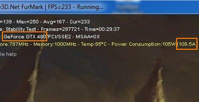
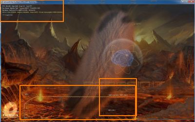
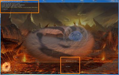
I just stress-tested with FurMark 1.9.0 my EVGA GTX 580 SC, overclocked at 900MHz with a Vcore (or VDDC or GPU voltage) of 1.100V. At first glance, the card was stable, no visual artifacts, a very high GPU temperature (96°C) with an insane power consumption: 385W for the card alone!

I even ran 3DMark11 without problem: P6534 and X2218.

I also launched Unigine Heaven 2.1 Direct3D 11 test (1920×1080, tessellation normal, 16X aniso, 4X MSAA): FPS: 52.9, Scores: 1333

But in Heaven, I noticed few visual artifacts. Then I launched an artifact scanning with the latest EVGA OC Scanner 1.6.0 and actually, 900MHz was a bit too high. Let’s see how to find stable and robust overclocking settings thanks to OC Scanner.


Test bench
- CPU: Core i7 960 @ 3.2GHz
- RAM: 4GB DDR3 Corsair Dominator
- Motherboard: GIGABYTE X58-A UD5
- Windows 7 64-bit
- Graphics drivers: R266.58
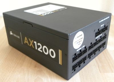
- PSU: Corsair AX1200

Corsair AX1200 power supply unit
A high quality PSU, like Corsair’s AX1200, is important for overclocking a high-end graphics card like the GTX 580


First thing to do for overclocking a GTX 580 is to disable the over current protection (OCP). I simply used the latest GPU-Z 0.5.1 with the /gtx500ocp option (for information, FurMark 1.9.0 makes this step simpler).

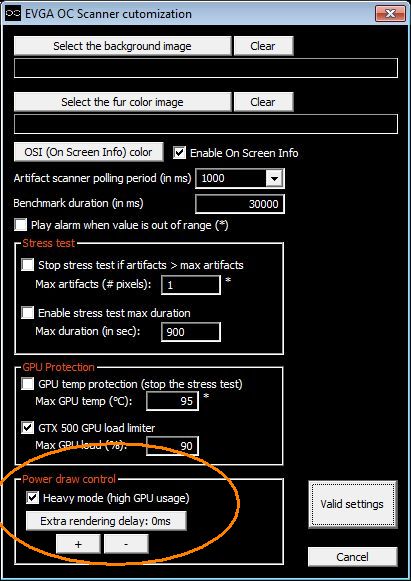
To detect artifacts with OC Scanner, I recommend to enable the heavy mode, in the settings box:

EVGA OC Scanner, settings box


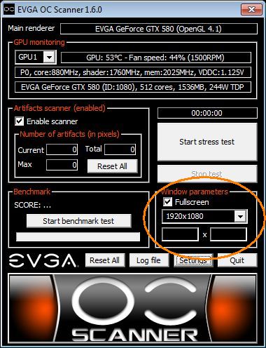
Then set the high resolution like 1920×1080 fullscreen:
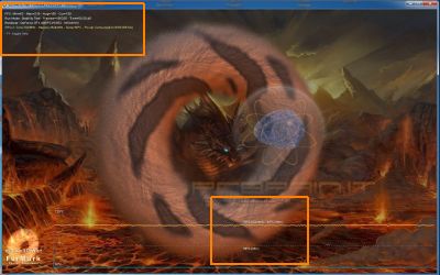
EVGA OC Scanner


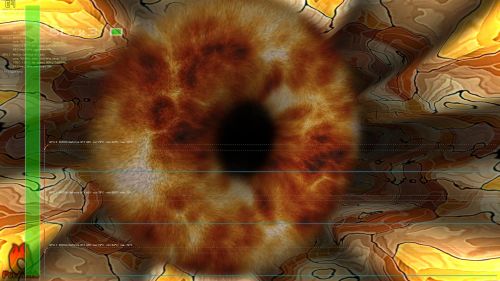
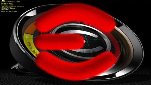
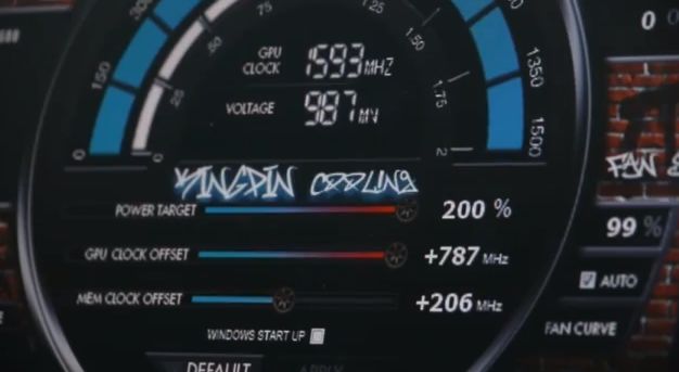
Okay OC Scanner is ready for artifacts scanning. Press the Start stress test button and you should see this rendering:

EVGA OC Scanner, GTX 580 SC


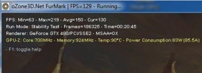
The most important line is the last one:

Artifacts: cur:0 - max:0 - total:0

In short, as long as all values are 0, that means you overclocking is stable. As soon as one value is greater than 0, your overclocking settings are too high:

EVGA OC Scanner artifacts, GTX 580 SC


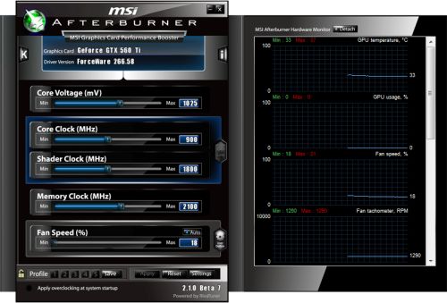
Here are the different steps of my GTX 580 overclocking (I set the core clock and core voltage with Afterburner 2.1.0 beta 7 –with Afterburner, 1.138V is the max GPU voltage we can set):

  • 1 – GPU @ 890MHz, VDDC @ 1.113V –> 4 artifacts dectected after 1 min
  • 2 – GPU @ 890MHz, VDDC @ 1.125V –> 2 artifacts dectected after 2 min
  • 3 – GPU @ 890MHz, VDDC @ 1.138V –> 2 artifacts dectected after 7 min
  • 4 – GPU @ 880MHz, VDDC @ 1.138V –> 1 artifact dectected after 4 min
  • 5 – GPU @ 880MHz, VDDC @ 1.125V –> 1 artifact dectected after 15 min
  • 6 – GPU @ 880MHz, VDDC @ 1.113V –> 1 artifact dectected after 3 min
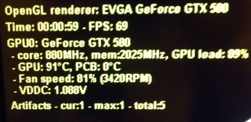
  • 7 – GPU @ 880MHz, VDDC @ 1.088V –> 5 artifacts detected after 1 min
  • 8 – GPU @ 870MHz, VDDC @ 1.088V –> 2 artifacts detected after 1 min
  • 9 – GPU @ 870MHz, VDDC @ 1.100V –> 1 artifact detected after 4 min
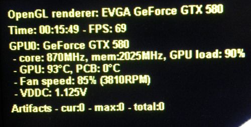
  • 10 – GPU @ 870MHz, VDDC @ 1.125V –> no artifact detected after 15 min

EVGA OC Scanner artifacts, GTX 580 SC


A you can see, OC Scanner is able to detect very small artifacts: few pixels in a full HD scene. Those few pixels are undetectable with our eyes in 3D scenes and that explains why I thought my OC was stable at 900MHz!

With these settings {870MHz, 1.125V}, the GPU temperature reaches 93°C and the power consumption of the testbed is 525W under OC Scanner. The power consumption of the testbed at idle is 120W and the PSU efficiency factor is around 0.9: (525-120) * 0.9 = 364W for the EVGA GTX 580 SC alone.

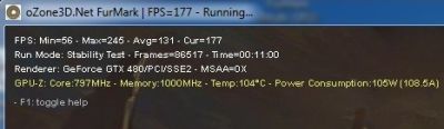
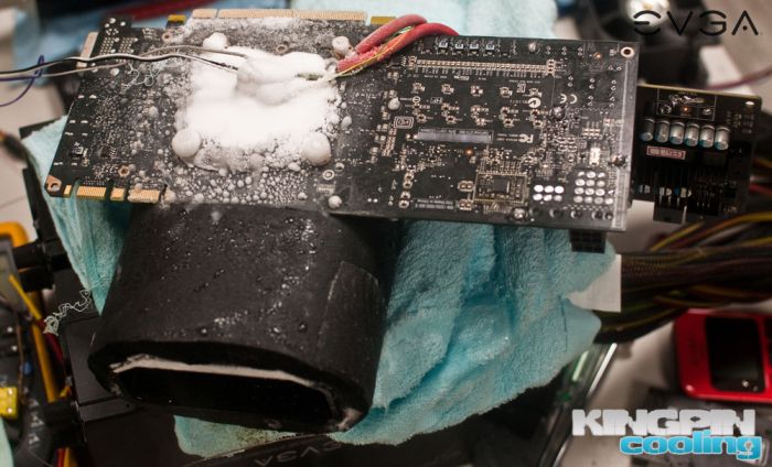
I validated these overclocking settings with a FurMark 1.9.0 burn-in test session (1920×1080 fullscreen, 15min): GPU: 98°C, fan speed 85% (3810RPM), total power consumption: 540W: (540-120)*0.9 = 378W for the GTX 580 alone!

EVGA GTX 580 SC, stress-tested by FurMark 1.9.0


378W ? Is it not too much? Sure my friend, it’s too much, this is even a very, ultra high value for the power consumption of a graphics card . NVIDIA says the TDP of a GTX 580 is… 240W. The GTX 580 has one 8-pin + one 6-pin power connectors leading to a max of 300W for the board (see here for more details: Maximum Power Consumption of Graphics Card Connectors). Then we are completely out of range with 378W! That’s why you have to have a solid PSU, a solid motherboard to overclock a high-end graphics card.

3DMark11 and Unigine Heaven scores with the new OC settings {870MHz, 1.125V}:
- 3DMark11: P6391
- Unigine Heaven 2.1: FPS: 51.7 , Scores: 1303

With a GPU core clocked at 870MHz and fed with a voltage of 1.125V, EVGA’s GTX 580 SC is stable. Finding the best overclocking settings for a GPU is a rather long process. And if you want to be sure that your OC settings are stable, I recommend you to burn your GPU with FurMark, or EVGA OC Scanner for at least one hour. After what, play with your favorite game to be sure the OC is okay.

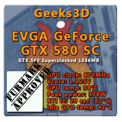
EVGA’s GTX 580 SC deserves this nice badge:

EVGA GTX 580 SC, FurMark approved!


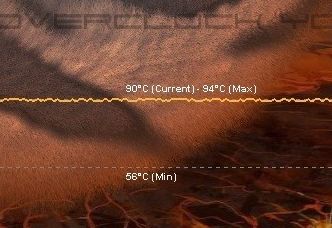
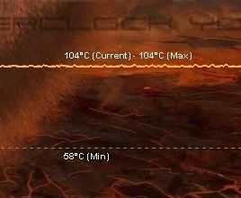
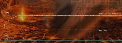
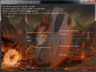
A detail about RTI tc. RTI tc is the Return To Idle time constant. This time constant is the time required for a reduction of 63% of the GPU temperature after a full loading (98°C is 100% and 42°C is the 0%). In our case, the system took 29 seconds to reach 62°C (decreasing of 63%). We can determine a kind of cooling factor:
(98-62) / 29 = 1.24 °C/sec.

GeForce GTX 590 Over Current Protection (OCP) and Overclocking

$
0
0

NVIDIA GeForce GTX 590


The R267.52 driver used by most of the reviewers for testing the GeForce GTX 590 does not offer a correct protection against over current especially when the GPU voltage is increased (see here: GTX 590 burns).

That’s why NVIDIA has released new drivers with a better OCP management: R267.84 and R287.85.

The default GPU voltage (or Vcore or VDDC) of the GTX 590 is around 0.93V (+/- 0.04V). NVIDIA recommends to not overvoltage the GPU (for example Vcore=1.200V) during overclocking. Here are NVIDIA’s guidelines for overclocking the HTX 590:

In the web release driver of GeForce GTX 590, we have added some important enhancements to our overcurrent protection for overclocking. We recommend anyone doing overclocking or running stress apps to always use the latest web driver to get the fullest protection for your hardware. Please note that overcurrent protection does not eliminate the risks of overclocking, and hardware damage is possible, particularly when overvoltaging. We recommend anyone using the GTX 590 board with the reference aircooler stick with the default voltage while overclocking, and avoid working around overcurrent protection mechanisms for stress applications. This will help maintain GTX 590′s great combination of acoustics, performance, and reliability. NVIDIA has worked with several watercooling companies to develop waterblocks for GTX 590, and these solutions will help provide additional margin for overclocking, but even in this case we recommend enthusiasts stay within 12.5-25mV of the default voltage in order to minimize risk.

These are guidelines only – any overclocking/overvoltaging can void your manufacturer’s product warranty.

At default voltage the GTX 590 is okay as NVIDIA said it to thinq.co.uk:

“Rest assured that the GTX 590 operates reliably at default voltages, and our 267.84 launch drivers provide additional levels of protection.”

[via]

EVGA Classified Test (X79 + 4-way SLI GTX 580 Ultra)

$
0
0

EVGA Classified X79 + GTX 580


k|ngp|n shows us his new toys in an classified overclocking session: an EVGA’s X79 Classified mobo, four EVGA’s GTX 580 Classified Ultra (a new model?) and no less than five 1200W Classified PSUs. The five 1200W PSUs are for a particular test, because only 2 of them are enough!

Some results:
- 3DMark 11 Performance score: P23160
- 3DMark 11 Extreme score: X9609

All pictures, scores and clock speeds are available HERE.

EVGA Classified X79 + GTX 580

EVGA Classified X79 + GTX 580

Radeon HD 7970 Quad CrossFire Scores (Air and LN2 Cooling)

$
0
0

Radeon HD 7970 Quad CrossFire, LN2 cooling


Tests with several Radeon HD 7970 appear everywhere on the Net these last days. VR-Zone has a test with four HD 7970 (air cooled) with stock clock speeds: 925MHz for the GPU and 1375MHz for the memory. The 3DMark 11 score in Performance and Extreme modes are: P23578 and X10233

Radeon HD 7970 Quad CrossFire
4-way CrossFire of air cooled HD 7970


For comparison, you can get around P7000 and X2500 with a good GTX 580…

But HD 7970 can be pushed further thanks to LN2 cooling (Liquid Nitrogen). With LN2, this guy has overclocked four HD 7970 at 1600MHz for the GPUs and 1880MHz for the memory modules. This overclocking gives the following P and X scores: P32234 and X18386

Current world records are around P27000 and X12000…

Radeon HD 7970 Quad CrossFire, LN2 cooling
4-way CrossFire of LN2 cooled HD 7970


Extreme OC Rig: EVGA GTX 680 Quad-SLI + X79 Classified

$
0
0

4-way SLI GeForce GTX 680 system


k|ngp|n’s latest LN2-ready system based on EVGA hardware (4-way SLI GeForce GTX 680 FTW –GPU @ 1900MHz– and X79 Classified mobo):

4-way SLI GeForce GTX 680 system

4-way SLI GeForce GTX 680 system

4-way SLI GeForce GTX 680 system


Source

k|ngp|n Smashes Three 3DMark 11 World Records with EVGA Hardware

$
0
0


With a ton of LN2 and GTX 680 Classified overclocked at close to 2100MHz, k|ngp|n has been able to break these 3DMark 11 records:

- 3DMark 11 Performance (Single Card) – P17,047
- 3DMark 11 Performance (2-Way SLI) – P25,380
- 3DMark 11 Extreme (4-Way SLI) – X17,384

EVGA GTX 680 Classified - Power target set to 200%
A power target set at 200% and a big offset in GPU core clock

FurMark 1.10.3 Released

$
0
0

FurMark, GPU stress test, burn-in utility


FurMark, the popular GPU burn-in utility, is back in a maintenance version. FurMark 1.10.3 adds the support of GTX 650 Ti, embeds the latest versions of GPU-Z and GPU Shark, and brings bugfixes.

FurMark 1.10.3 DOWNLOAD

You can download FurMark 1.10.3 here:
Webmasters: hotlinking is not allowed, please use the post url as download link.
Download FurMark 1.10.3 Version 1.10.3


FurMark 1.10.3 changelog

  • Update: support of NVIDIA GeForce GTX 650 Ti.
  • Update: GPU-Z 0.6.6 and GPU Shark 0.6.7
  • Update: ZoomGPU 1.8.10 (GPU monitoring library).
  • Bugfix: Offsets for GPU core and memory added to base and boost clocks for GTX 600.
  • Bugfix: benchmark scores: average FPS was in some case lower than min FPS.

FurMark, GPU stress test, burn-in utility

MSI Kombustor 2.5.0 Released

$
0
0

MSI Kombustor 2.5.0, GeForce OC Test
MSI Kombustor, GF OC Test


MSI Kombustor has been updated to version 2.5.0. This new release includes a new 3D test, updates Kombustor loader for Windows 8 (KLoaderWin32.exe) and takes account the offsets for core and memory clock speeds on GeForce GTX 600 series. The latest version of GPU Shark has been embedded too.

The new 3D test, called GF OC Test is a simple OpenGL 4 tessellation test for quickly checking the OC settings of a GeForce GTX 600 card. Indeed, if the GPU core clock is too high, this new test fails immediately (and you have to kill it with the task manager). TessMark or Ungine Heaven behave the same way.


You can download MSI Kombustor 2.5.0 here (left-click to grab the file):
Download MSI Kombustor 2.5.0 Version 2.5.0


You can post your feedbacks or bug reports in the following places: Afterburner forum or in the comments section of this article.

MSI Kombustor 2.5.0
MSI Kombustor main interface

MSI Kombustor 2.4.2
MSI Kombustor, burn-in test

MSI Kombustor 2.4.2
MSI Kombustor, PhysX + tessellation + geometry instancing test

Zotac FireStorm Graphics Card Overclocking Utility v2.01

$
0
0

Zotac FireStorm Graphics Card Overclocking Utility


Zotac has released a new version of FireStorm, its overclocking utility for graphics cards. This new version of FireStorm comes with a new user-friendly interface as well as some new overclocking and monitoring features. FireStorm is not limited to Zotac cards, I tested it with my MSI GTX 660 Hawk without notable problem:

Zotac FireStorm Graphics Card Overclocking Utility

Zotac FireStorm Graphics Card Overclocking Utility

Zotac FireStorm Graphics Card Overclocking Utility


I must say that I’m not a big fan of all those skins that generates enormous user interfaces. Just look at the difference between GPU-Z and FireStorm:

Zotac FireStorm Graphics Card Overclocking Utility

More information about FireStorm 2.01: ZOTAC Releases New FireStorm Overclocking Utility.


Download: FireStorm videocard overclocking utility.


ZOTAC FireStorm from ZOTAC on Vimeo.

via

Viewing all 30 articles
Browse latest View live


<script src="https://jsc.adskeeper.com/r/s/rssing.com.1596347.js" async> </script>